- 您现在的位置:买卖IC网 > Sheet目录3875 > PIC16C55A-04/P (Microchip Technology)IC MCU OTP 512X12 28DIP
2002 Microchip Technology Inc.
Preliminary
DS30453D-page 37
PIC16C5X
8.0
TIMER0 MODULE AND TMR0
REGISTER
The Timer0 module has the following features:
8-bit timer/counter register, TMR0
- Readable and writable
8-bit software programmable prescaler
Internal or external clock select
- Edge select for external clock
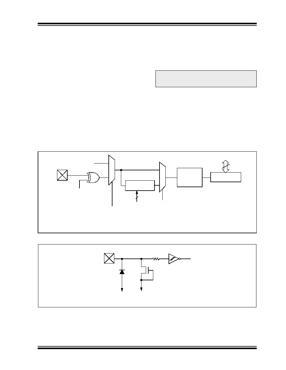
Figure 8-1 is a simplified block diagram of the Timer0
module, while Figure 8-2 shows the electrical structure
of the Timer0 input.
Timer mode is selected by clearing the T0CS bit
(OPTION<5>). In Timer mode, the Timer0 module will
increment every instruction cycle (without prescaler). If
TMR0 register is written, the increment is inhibited for
the following two cycles (Figure 8-3 and Figure 8-4).
The user can work around this by writing an adjusted
value to the TMR0 register.
Counter mode is selected by setting the T0CS bit
(OPTION<5>). In this mode, Timer0 will increment
either on every rising or falling edge of pin T0CKI. The
incrementing edge is determined by the source edge
select bit T0SE (OPTION<4>). Clearing the T0SE bit
selects the rising edge. Restrictions on the external
clock input are discussed in detail in Section 8.1.
The prescaler assignment is controlled in software by
the control bit PSA (OPTION<3>). Clearing the PSA bit
will assign the prescaler to Timer0. The prescaler is not
readable or writable. When the prescaler is assigned to
the Timer0 module, prescale values of 1:2, 1:4,...,
1:256 are selectable. Section 8.2 details the operation
of the prescaler.
A summary of registers associated with the Timer0
module is found in Table 8-1.
FIGURE 8-1:
TIMER0 BLOCK DIAGRAM
FIGURE 8-2:
ELECTRICAL STRUCTURE OF T0CKI PIN
Note:
The prescaler may be used by either the
Timer0 module or the Watchdog Timer, but
not both.
Note 1: Bits T0CS, T0SE, PSA, PS2, PS1 and PS0 are located in the OPTION register
2: The prescaler is shared with the Watchdog Timer (Figure 8-6).
T0CKI
T0SE(1)
0
1
0
pin
T0CS(1)
FOSC/4
Programmable
Prescaler(2)
Sync with
Internal
Clocks
TMR0 reg
PSout
(2 cycle delay)
PSout
Data Bus
8
PSA(1)
PS2, PS1, PS0(1)
3
Sync
VSS
RIN
Schmitt Trigger
N
Input Buffer
T0CKI
pin
Note 1: ESD protection circuits.
(1)
发布紧急采购,3分钟左右您将得到回复。
相关PDF资料
DSPIC30F3014T-20I/PT
IC DSPIC MCU/DSP 24K 44TQFP
DSPIC30F3014T-20I/ML
IC DSPIC MCU/DSP 24K 44QFN
PIC16LF819T-I/MLTSL
IC PIC MCU FLASH 2KX14 28QFN
PIC16LF819T-I/SOTSL
IC PIC MCU FLASH 2KX14 18SOIC
PIC18LF8410T-I/PT
IC PIC MCU FLASH 8KX16 80TQFP
PIC18F2410T-I/ML
IC PIC MCU FLASH 8KX16 28QFN
PIC18F2331T-E/SOG
IC PIC MCU FLASH 4KX16 28SOIC
PIC18F4331T-I/ML
IC MCU FLASH 4KX16 44QFN
相关代理商/技术参数
PIC16C55A-04/P
制造商:Microchip Technology Inc 功能描述:IC 8BIT CMOS MCU 16C55 DIP28
PIC16C55A-04/P
制造商:Microchip Technology Inc 功能描述:Microcontroller IC Number of I/Os:20
PIC16C55A-04/SO
功能描述:8位微控制器 -MCU .75KB 24 RAM 20 I/O 4MHz SOIC-28 RoHS:否 制造商:Silicon Labs 核心:8051 处理器系列:C8051F39x 数据总线宽度:8 bit 最大时钟频率:50 MHz 程序存储器大小:16 KB 数据 RAM 大小:1 KB 片上 ADC:Yes 工作电源电压:1.8 V to 3.6 V 工作温度范围:- 40 C to + 105 C 封装 / 箱体:QFN-20 安装风格:SMD/SMT
PIC16C55A-04/SO
制造商:Microchip Technology Inc 功能描述:8BIT CMOS MCU SMD 16C55 SOIC28
PIC16C55A-04/SP
功能描述:8位微控制器 -MCU .75KB 24 RAM 20 I/O 4MHz SPDIP-28 RoHS:否 制造商:Silicon Labs 核心:8051 处理器系列:C8051F39x 数据总线宽度:8 bit 最大时钟频率:50 MHz 程序存储器大小:16 KB 数据 RAM 大小:1 KB 片上 ADC:Yes 工作电源电压:1.8 V to 3.6 V 工作温度范围:- 40 C to + 105 C 封装 / 箱体:QFN-20 安装风格:SMD/SMT
PIC16C55A-04/SS
功能描述:8位微控制器 -MCU .75KB 24 RAM 20 I/O 4 MHz SSOP-28 RoHS:否 制造商:Silicon Labs 核心:8051 处理器系列:C8051F39x 数据总线宽度:8 bit 最大时钟频率:50 MHz 程序存储器大小:16 KB 数据 RAM 大小:1 KB 片上 ADC:Yes 工作电源电压:1.8 V to 3.6 V 工作温度范围:- 40 C to + 105 C 封装 / 箱体:QFN-20 安装风格:SMD/SMT
PIC16C55A-04E/P
功能描述:8位微控制器 -MCU .75KB 24 RAM 20 I/O RoHS:否 制造商:Silicon Labs 核心:8051 处理器系列:C8051F39x 数据总线宽度:8 bit 最大时钟频率:50 MHz 程序存储器大小:16 KB 数据 RAM 大小:1 KB 片上 ADC:Yes 工作电源电压:1.8 V to 3.6 V 工作温度范围:- 40 C to + 105 C 封装 / 箱体:QFN-20 安装风格:SMD/SMT
PIC16C55A-04E/SO
功能描述:8位微控制器 -MCU .75KB 24 RAM 20 I/O RoHS:否 制造商:Silicon Labs 核心:8051 处理器系列:C8051F39x 数据总线宽度:8 bit 最大时钟频率:50 MHz 程序存储器大小:16 KB 数据 RAM 大小:1 KB 片上 ADC:Yes 工作电源电压:1.8 V to 3.6 V 工作温度范围:- 40 C to + 105 C 封装 / 箱体:QFN-20 安装风格:SMD/SMT